Spatial Development Route
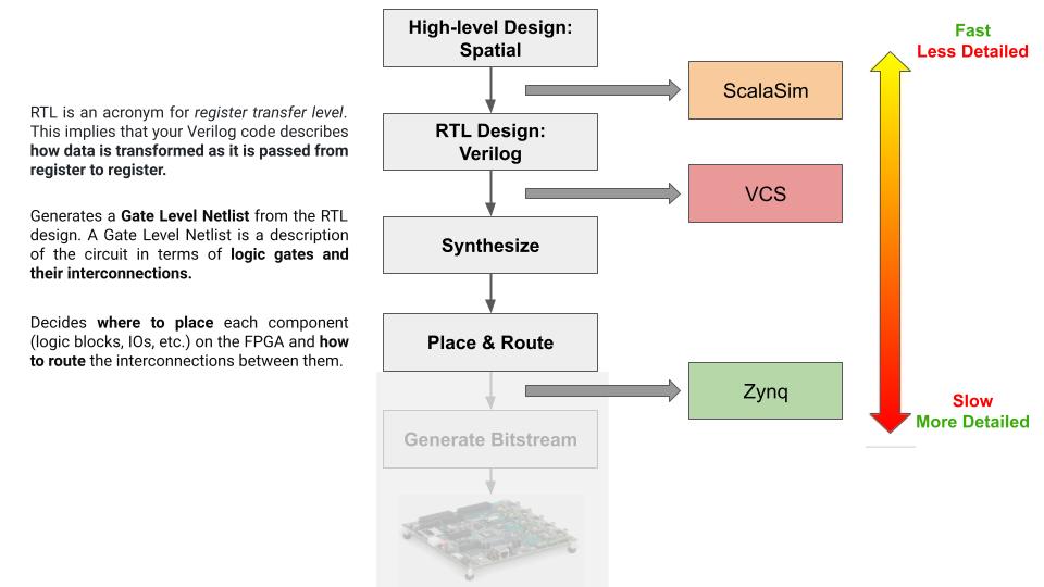
When using Spatial and its supported simulation backends to design your hardware, you will follow a design flow that is shown in this diagram. If you are not familiar with concepts such as RTL, Logic Synthesis, and Placement and Routing, please read throught the explanation of each step and terminonlogy in the diagram below.

For the scope of this course, you are required to synthesize and do the placement and routing of your design. More details on how to lower your design and conduct logic synthesis, placemane and routing will be introduced in the following sections together with instructions on how to run simulation in each step. (We will not require you to actually run it on a actual FPGA.)
There are three simulations provided to help you check the correctness and improve performance of your design.
-
Scalasim: This is the simulation we have used so far for the labs. It is much faster than the other two backends (VCS and ZCU) as it does not generate the Verilog desciption of your design and run synthesis. Therefore, the fast speed comes with the cost that it maybe less accurate and may not provide all the low-level profiling details of your design. However, it reports estimates of the resource utilization for your application and it can serve as a useful profiling tool that will help you to iterate over many designs in the early stage of your project.
Known issues on Scalasim: read this section
-
VCS: Unlike Scala simulation, VCS simulation generates RTL description (this will be in Verilog) of your design. Compared to Scala simulation, VCS simulation takes longer to complete (because the circuit needs to be simulated at every clock cycle), but it gives a simulation environment that's more similar to what will be running on the board. For example, you can have a design that passes the Scala simulation, but fails the VCS simulation because the circuit that gets generated is not correct.
NOTE: VCS and ZCU uses licensed software such as VCS and Vivado. We have these installed in the lagos server, so if you want to run these simulations, log into the lagos server with your SUID.
-
ZCU: While the VCS simulation will generate the RTL description and do a cycle-accurate simulation on it, it does not do the logic synthesis and placement and routing. This backend will lower further from your RTL description and will target the Xilinx ZCU102 FPGA by conducting synthesis and placement and routing. This will give you detailed reports of your design's resource utilization on the target FPGA.
NOTE: VCS and ZCU uses licensed software such as VCS and Vivado. We have these installed in the lagos server, so if you want to run these simulations, log into the lagos server with your SUID.
Scalasim
How to run Scalasim simulation
You can run the scala simulation by running the following command (you should replace $PROJECT_DIRECTORY and $TEST_NAME):
cd $PROJECT_DIRECTORY  # Change this to your project directory
sbt -Dtest.CS217=true "; testOnly $TEST_NAME"
Simulation reports
Cycle Count
After running your application, artifacts will be generated into gen/CS217/$TEST_NAME. The most important files are:
SimulatedExecutionSummary_*.log: This captures the cycle count and trip count of each controllerinfo/PostExecution.html: This contains an html-based information dump of the cycle count of each controller
Both of the files show the line of code for each controller, so you can use this information to match it with your code. For example, in lab1's Lab1Part2DramSramExample, you can use the SimulatedExecutionSummary_*.log to understand how long each parts of your codeo took like this:


For more detailed information, you can look at info/PostExecution.html. It contains informations such as initiaion interval and latency for the Foreach loops. (If you are not familiar with initiation interval or pipelining, read this.)
Resource Utilization
Scalasim also gives you a rough estimate of the resource utilization of your application. Whenever you run a simulation, a Main.json file will be created under gen/CS217/$TEST_NAME/reports/. For example, the file for Lab1Part2DramSramExample in Lab 1 will look like:
{
	"bram": {
		"x224_b1_0": [32, [16], [0], 1],
		"x245_b2_0": [32, [16], [0], 1]
	},
	"fixed_ops": 5
}
You can also use the provided python script computeResourceUtilization.py which summarizes the resource utilization in a more concise manner. Run the following script with the proper $file_name. (Note: Memory sizes in this output are given in bits, not bytes)
python computeResourceUtilization.py $file_name
# ex: python computeResourceUtilization.py gen/CS217/Lab1Part2DramSramExample/reports/Main.json
Test Results
Terminal If you succeeded running the simulation, the terminal will let you know.
SimulatedExecutionLog_*.log
You can find this file under the gen/CS217/$TEST_NAME folder. This captures the print statements in your test case
VCS
How to run VCS simulation
You can run the VCS simulation by running the following command (you should replace $PROJECT_DIRECTORY and $TEST_NAME):
cd $PROJECT_DIRECTORY
source exports.sh
sbt -Dtest.VCS=true "; testOnly $TEST_NAME"
For VCS and ZCU backend, you will have to set several environment variables using the source exports.sh command. Use the expoerts.sh file placed in lab3's skeleton repository.
Simulation reports
Cycle Count
To see the cycle count for the controllers, open the gen/VCS/$TEST_NAME/info/controller_tree.html.
Resource Utilization
N/A (To get the resource utilization information, you need to do placement and routing, which happens in the synthesis step.)
Test Results
Terminal
If you succeeded running the simulation, the terminal will let you know.

run.log
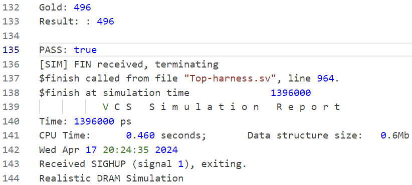
To view the results of the print statements you inserted, open the logs/VCS/$TEST_NAME/run.log.
Tip: If you're using Visual Studio Code IDE, hovering your mouse over the file name in the line
Backend run in $PROJECT_DIRECTORY/./logs/VCS/$TEST_NAME//run.logand doingctrl + clickwill directly open the file for you.
At the end of the file, you will be able to see the print statements in your tests (line 132-135 in the picture below).

ZCU
How to run the ZCU backend
cd $PROJECT_DIRECTORY
source exports.sh
sbt -Dtest.ZCU=true "; testOnly $TEST_NAME"
For VCS and ZCU backend, you will have to set several environment variables using the source exports.sh command. Use the expoerts.sh file placed in lab3's skeleton repository.
The synthesis process would take 30 min ~ 1 hour to run.
Known issues during synthesis
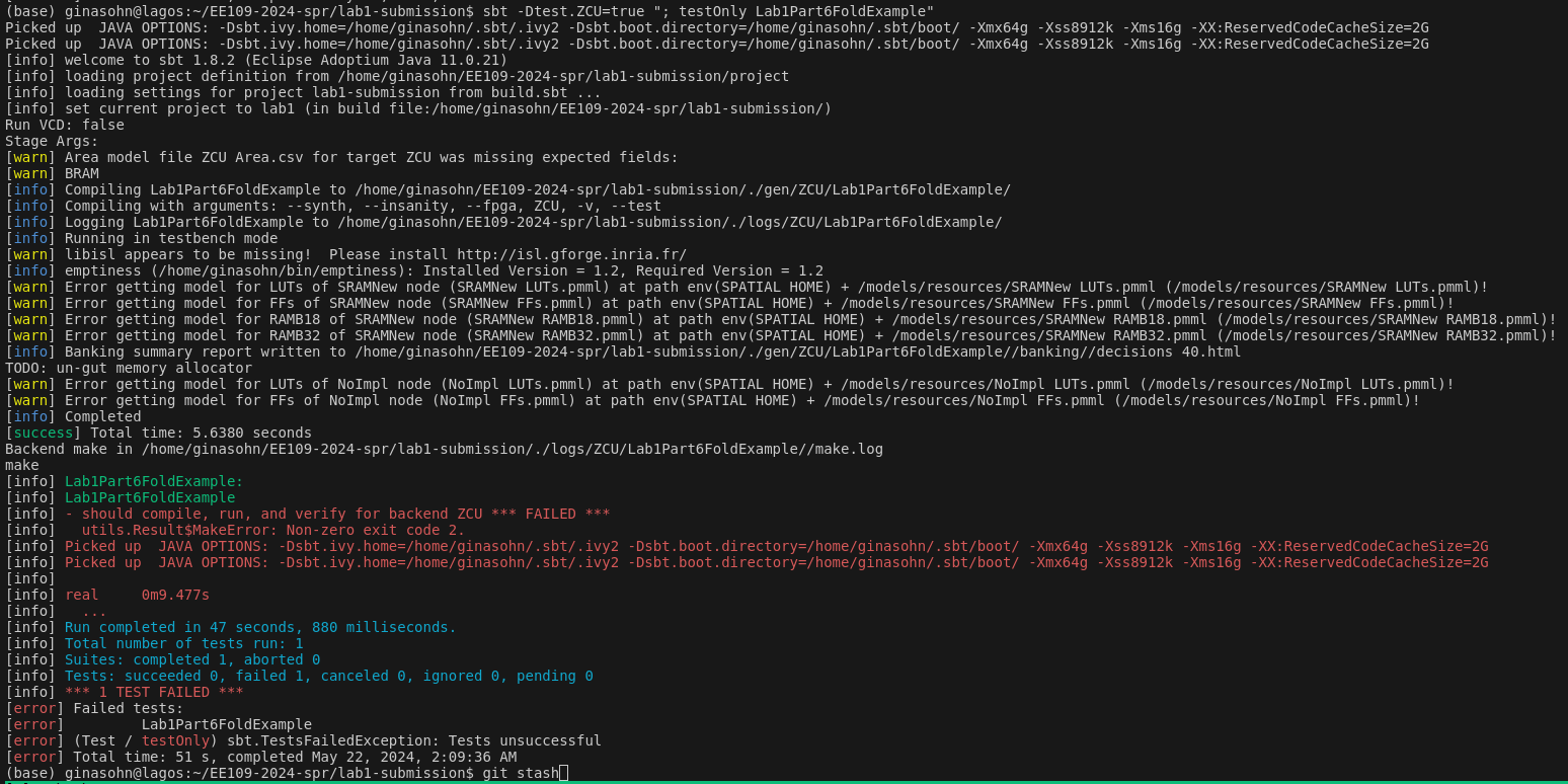
When running synthesis, there are some issues with building the host software. So you will see an error message in the terminal that looks like:

However, this does not affect the synthesis stage of your hardware design. Check if the end.log file has been properly created under gen/ZCU/$TEST_NAME/. The end.log contains the timestamp when the hardware synthesis is completed (this will usually be a 10-digit number). If you can find this file and can see the resource utilization report, then your hardware design has been successfully synthesized. The following section will explain how to see the resource utilization report.
Synthesis reports
Resource Utilization
After the synthesis finishes, you will have access to the report of your design's resource utilization on the target FPGA. The report is located in gen/$TEST_NAME/verilog-zcu/. The resource utilization report is named par_utilization.rpt.
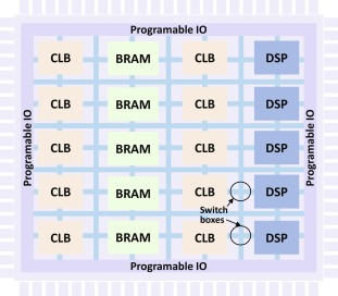
The figure below shows the basic FPGA structure that consists of an array of:
- configurable logic blocks (CLBs): Programmable logic cells. LUTs, Registers and computations that are not executed in the DSP will be mapped to these blocks.
- block RAMs (BRAMs)
- digital signal processing (DSP) blocks: These execute compute-intensive operations such as multiply-and-accumulate (MAC)
- programmable interconnection networks
- a set of programmable input and output pads around the device
 (ref: https://www.sciencedirect.com/science/article/pii/S0065245820300899)
You can access how much of the resources your design is using by looking at the following sections in the report par_utilization.rpt:
-
CLB Logic
+--------------------------------------+------+-------+-----------+-------+ | Site Type | Used | Fixed | Available | Util% | +--------------------------------------+------+-------+-----------+-------+ | CLB LUTs | 6107 | 0 | 274080 | 2.23 | | LUT as Logic | 4375 | 0 | 274080 | 1.60 | | LUT as Memory | 882 | 0 | 144000 | 0.61 | | LUT as Distributed RAM | 808 | 0 | | | | LUT as Shift Register | 74 | 0 | | | | LUT used exclusively as pack-thrus | 850 | 0 | 274080 | 0.31 | | CLB Registers | 6721 | 0 | 548160 | 1.23 | | Register as Flip Flop | 6721 | 0 | 548160 | 1.23 | | Register as Latch | 0 | 0 | 548160 | 0.00 | | Register as pack-thrus | 0 | 0 | 548160 | 0.00 | | CARRY8 | 186 | 0 | 34260 | 0.54 | | F7 Muxes | 33 | 0 | 137040 | 0.02 | | F8 Muxes | 1 | 0 | 68520 | <0.01 | | F9 Muxes | 0 | 0 | 34260 | 0.00 | +--------------------------------------+------+-------+-----------+-------+ -
BLOCKRAM
 +-------------------+------+-------+-----------+-------+
 |     Site Type     | Used | Fixed | Available | Util% |
 +-------------------+------+-------+-----------+-------+
 | Block RAM Tile    |   15 |     0 |       912 |  1.64 |
 |   RAMB36/FIFO*    |   14 |     0 |       912 |  1.54 |
 |     RAMB36E2 only |   14 |       |           |       |
 |   RAMB18          |    2 |     0 |      1824 |  0.11 |
 |     RAMB18E2 only |    2 |       |           |       |
 +-------------------+------+-------+-----------+-------+
For a more detailed report on the on-chip memory requirements of your design, see the
par_ram_utilization.rptfile. In the summary section, you will be able to see a table like this and there are also other sections such as Utilization, Performance, Power for the memory components:+--------------------------+------------+-----------+--------+------------+ | Memory Type | Total Used | Available | Util % | Inferred % | +--------------------------+------------+-----------+--------+------------+ | URAM | 0.0 | 0 | 0.0 | 0.0 | | BlockRAM | 0.0 | 912 | 0.0 | 0.0 | | LUTMs as Distributed RAM | 101.0 | 144000 | 0.1 | 100.0 | | LUTMs as RAM64M8 | 9 | | | 100.0 | | LUTMs as RAM32M16 | 92 | | | 100.0 | +--------------------------+------------+-----------+--------+------------+ -
ARITHMETIC: This explains how much of the DSP logics your design is using.
 +----------------+------+-------+-----------+-------+
 |    Site Type   | Used | Fixed | Available | Util% |
 +----------------+------+-------+-----------+-------+
 | DSPs           |   42 |     0 |      2520 |  1.67 |
 |   DSP48E2 only |   42 |       |           |       |
 +----------------+------+-------+-----------+-------+
For students that are trying to draw a roofline model for their application:
-
Reasoning about FLOPS:
-
For FLOPS, you should look at your DSP utilization and the utilization of 'LUT as Logic' in the CLB section.
-
[DSP] The DSP48E2 is a Digital Signal Processing (DSP) slice commonly used in Xilinx FPGAs, such as those in the Virtex UltraScale+ family. The number of Floating Point Operations per Second (FLOPS) that a DSP48E2 can execute depends on the specific configuration and clock frequency at which it operates.
- Operations per Cycle: A single DSP48E2 slice can perform a multiply-accumulate operation (MAC) in one clock cycle. This involves two multiplications and one addition/subtraction, which is typically considered as two floating-point operations (FLOPs) per cycle (one multiplication and one addition).
- Clock Frequency: The maximum clock frequency of a DSP48E2 slice can vary depending on the FPGA model and operating conditions. You can find the clock frequency in the
gen/$TEST_NAME/verilog-zcu/parClockFreq.shfile. - To estimate the FLOPS, you can use the following formula. I will use an example where each DSP48E2 slice is running at 500 MHz and the FPGA has 4000 DSP48E2 slices.

-
[CLB] 'LUT as Logic' in the CLB section indicates the number of LUTs that are being used purely to implement combinational logic. Combinational logic refers to logic circuits whose output is a pure function of the present input only, without any memory or feedback (e.g., AND, OR, XOR gates). As this can be configured to execute various kinds of combinational logic, it is hard to reason about FLOPS precisely. Therefore, you can try to tie them in to your roofline model by creating a metric based on the number of blocks available for
LUT as Logic.
-
-
Reasoning about Bandwidth: When drawing a roofline, you can use different memory bandwidths depending on where you are drawing the boundaries in your system. However, the common bandwidth you would use will propably be the bandwidth of the off-chip DRAM. For this, you can look up the bandwidth of a DDR4 DRAM.
If you would like to learn more about the report, watching this video will be helpful. (The video uses 'Slice' instead of 'CLB', but you can think of them similarly.)
Difference between 'Slice' and 'CLB'
In the context of FPGA design, particularly when using Xilinx FPGAs and the Vivado design suite, the terms "slice" and "Configurable Logic Block (CLB)" refer to specific components of the FPGA architecture.
- Configurable Logic Block (CLB):
- A CLB is a fundamental building block of Xilinx FPGA architectures. It comprises several finer-grain components that provide the logic capabilities of the FPGA.
- Typically, a CLB contains multiple slices (the exact number can vary based on the specific FPGA family), and these slices are the elements that actually implement the logic.
- Each CLB is designed to perform a wide array of functions, which include combinational logic (like AND, OR, NOT operations) and sequential logic (like flip-flops or latches).
- Slice:
- A slice is a part of a CLB and acts as the smallest unit of logic within the FPGA structure in Xilinx devices.
- Each slice typically contains a set of Look-Up Tables (LUTs), flip-flops, and multiplexers.
In summary, the main difference lies in the hierarchy and scale of functionality: a CLB is a larger structural unit in an FPGA that contains multiple slices, which are the actual implementers of logic. The CLB coordinates the operations of its constituent slices to execute complex logic and storage operations. In Vivado, you'll often deal with both terms when defining and analyzing the physical layout and logical implementation of your FPGA designs.
Known Issue
Scalasim: line buffers
Scalasim can simulate the building blocks we have used so far in the labs except for line buffers. Unfortunately, Scalasim cannot properly simulate the line buffer, so if you want to use line buffers, you will have to simulate it with VCS like how we did in lab3.
Using Math Functions
For math functions such as power, exponential, cos, sin, random number generation, etc., you have to implement them manually in your accelerator design or generate the numbers that use this in the host code region and read them in.
If you would like to implement the math functions in your accelerator design, consider either one of the following methods. Both algorithms will be an approximation; For CORDIC, you adjust the number of itertions and for Taylor Expansion, you adjust the number of terms for accuracy. Therefore, make sure what is the level of precision your application requires and check whether your implementation does not affect the correctness / quality of your application:
- CORDIC Algorithm
- CORDIC Basics
- Learn CORDIC with Chatgpt: I (Gina) am also new to using CORDIC to implement math functions. I used chatgpt to get a first grasp of what the algorithm is and how I implement it, which ended up being quite useful. I collected parts of the responses I got from ChatGPT in this doc. Hope this helps some of you who are also new to CORDIC.
- Taylor Expansion:
Some Pros and Cons for each methods:
-
CORDIC Algorithm
- Pros:
- Hardware Efficiency: No Multipliers Needed. CORDIC only requires addition, subtraction, bit-shifting, and look-up tables, making it very efficient in terms of hardware resources.
- Versatility: CORDIC can compute a wide range of functions, including trigonometric, hyperbolic, exponential, and logarithmic functions, as well as square roots.
- Iterative Refinement: The precision can be easily adjusted by changing the number of iterations, without having to change the euqation you are implementing.
- Cons:
- CORDIC Gain: The CORDIC gain (Scaling Factor) must be accounted for in the final result, adding an additional step to the computation.
- Precomputed Values: Requires precomputed angle values stored in look-up tables, which consume some memory resources.
- Pros:
-
Taylor Series
- Pros:
- Simplicity for Specific Functions: For certain functions, Taylor series can provide a direct and straightforward method for approximation. The mathematical foundation is easier to understand and implement for specific functions.
- Accuracy for Small Intervals: For small intervals around the expansion point, the Taylor series can provide high accuracy with a few terms.
- Cons:
- Resource Intensive: Higher-order terms require multipliers, which can be resource-intensive on FPGAs.
- Range of Convergence: The Taylor series is accurate only within a certain range around the expansion point. For values outside this range, the accuracy diminishes quickly.
- Non-Iterative Nature: If you want to increase the number of terms for better accuracy, the equation you will have to implement will change.
- Pros: